Surface Mount Devices (SMDs) are electronic components mounted directly onto the surface of a printed circuit board (PCB). Their small size has become integral to the efficiency of electronic devices.
Let’s start by exploring the benefits of SMDs, as opposed to traditional through-holes:
| Benefit | Description |
| :=== | :=== |
| Miniaturization | SMDs enable electronic miniaturization, crucial for space-constrained applications. |
| High-Density Assembly | SMDs allow for high-density PCB assembly, optimizing component placement for increased overall density. |
| Improved Electrical Performance | Shorter lead lengths in SMDs reduce parasitic elements, enhancing high-frequency performance and signal integrity. |
| Reduced Signal Interference | Compact size and direct PCB placement minimize loop areas, reducing electromagnetic interference EMI. |
| Automated Manufacturing | SMDs are compatible with automated pick-and-place, ensuring efficient and precise mass production with cost savings. |
| Lower Weight and Cost | SMDs contribute to lighter devices, and automated assembly reduces manufacturing costs.|
| Enhanced Thermal Performance | SMDs with exposed metal pads improve thermal dissipation, enhancing overall thermal performance. |
| Better Mechanical Stability | SMDs, soldered directly to PCBs, provide superior mechanical stability, making them more resistant to shocks, vibrations, and mechanical stresses. |
SMD Packaging for Passive Components
Surface Mount Device (SMD) packaging for passive components, such as resistors, capacitors, and inductors, involves a variety of package types:
Chip Resistors and Capacitors (Standard Ceramic Packages)
Packages: The most common SMD package for chip resistors and capacitors is the ceramic chip package. It comes in various standardized sizes, such as 0402, 0603, 0805, and 1206.
Materials: Typically made of ceramic materials with conductive layers for electrodes and dielectric layers for capacitors.
Advantages: Compact size, suitable for high-density applications.
Tantalum Capacitors
Packages: Tantalum capacitors come in SMD packages like the molded tantalum chip (MTC) and molded tantalum leadframe (MTL) packages.
Materials: Tantalum-based dielectric material with a metal case for encapsulation.
Advantages: Higher capacitance values in a compact size, suitable for applications requiring stable capacitance over a wide temperature range.
Aluminum Electrolytic Capacitors
Packages: SMD aluminum electrolytic capacitors are available in various configurations, including cylindrical and chip-type packages.
Materials: Aluminum-based electrolyte with a metallic case.
Advantages: Larger capacitance values compared to ceramic capacitors, suitable for applications requiring higher energy storage.
Multilayer Ceramic Capacitors (MLCC)
Packages: MLCCs are available in various standard sizes, including 0402, 0603, 0805, 1206, and larger.
Materials: Multilayered ceramic structure with alternating layers of ceramic and conductive material.
Advantages: High capacitance density, suitable for high-frequency applications and decoupling.
SMD Packaging for Active Components
| Category | Package | Types | Materials | Advantages |
| :=== | :=== | :=== | :=== | :=== |
| Transistors | SOT (Small Outline Transistor) | SOT-23, SOT-89, SOT-223 | Plastic or epoxy resin with metal leads | Compact size, suitable for low to medium-power discrete transistors |
| Integrated Circuits (ICs) | QFN (Quad Flat No-Lead) | Compact, leadless with exposed thermal pad on the bottom | Plastic or ceramic with metal leads/pads | Compact, suitable for high-density integration, various pin counts, and configurations |
| | TQFP (Thin Quad Flat Package) | Flat, square-shaped with gull-wing leads | | |
| | SOIC (Small Outline Integrated Circuit) | Small, rectangular with gull-wing leads | | |
| | SSOP (Shrink Small Outline Package) | Similar to SOIC but with a smaller body size | | |
| Microcontrollers | LQFP (Low-profile Quad Flat Package) | Common sizes: 32, 48, 64, 100 pins | Plastic or ceramic with gull-wing leads | Good balance between size and ease of soldering, suitable for microcontroller applications |
| Ball Grid Array (BGA) | BGA (Ball Grid Array) | PBGA (Plastic BGA), CBGA (Ceramic BGA) | Plastic or ceramic with solder balls | High pin count, compact design, excellent thermal performance, suitable for high-performance applications |
| Chip-on-Board (COB) | COB (Chip-on-Board) | Bare semiconductor chips mounted on PCB, wire bonding | Semiconductor chips and wire bonds | Compact, cost-effective for high-volume applications, flexibility in design |
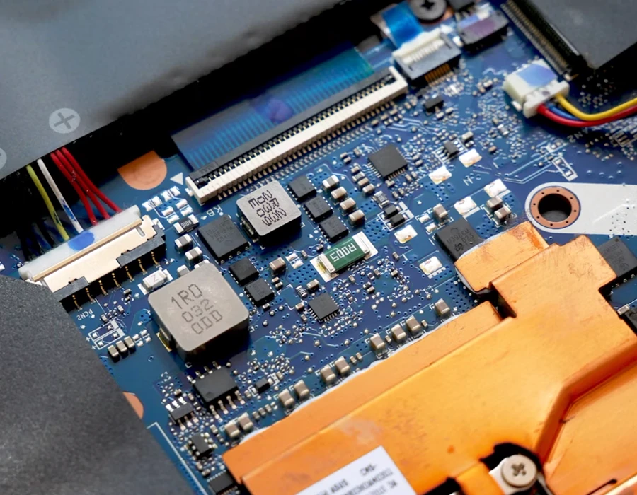
Motherboard utilizing surface mount technology
Challenges with Surface Mount Devices
SMDs come with their own set of challenges during assembly and use:
Tombstoning: Tombstoning occurs when one end of a passive SMD component is vertically displaced during reflow soldering, resembling a tombstone. This anomaly may arise from uneven heating profiles, inadequacies in solder paste deposition, or irregularities in component placement precision.
Solder Bridging: Solder bridging involves unintended connections between adjacent pads, leading to short circuits. Root causes include excessive solder paste application, suboptimal stencil design, or inadequate implementation of solder mask features.
Skew and Misalignment: Skew and misalignment issues materialize when SMD components deviate from precise placement on PCB pads during the pick-and-place process. These discrepancies can result in compromised solder joints and consequential performance degradation.
Insufficient Solder Joints: Incomplete or inadequate solder joints may occur due to factors such as insufficient solder paste deposition, suboptimal reflow soldering conditions, or inaccuracies in component placement. These deficient joints can yield intermittent electrical connections or outright failures.
Let’s start by exploring the benefits of SMDs, as opposed to traditional through-holes:
| Benefit | Description |
| :=== | :=== |
| Miniaturization | SMDs enable electronic miniaturization, crucial for space-constrained applications. |
| High-Density Assembly | SMDs allow for high-density PCB assembly, optimizing component placement for increased overall density. |
| Improved Electrical Performance | Shorter lead lengths in SMDs reduce parasitic elements, enhancing high-frequency performance and signal integrity. |
| Reduced Signal Interference | Compact size and direct PCB placement minimize loop areas, reducing electromagnetic interference EMI. |
| Automated Manufacturing | SMDs are compatible with automated pick-and-place, ensuring efficient and precise mass production with cost savings. |
| Lower Weight and Cost | SMDs contribute to lighter devices, and automated assembly reduces manufacturing costs.|
| Enhanced Thermal Performance | SMDs with exposed metal pads improve thermal dissipation, enhancing overall thermal performance. |
| Better Mechanical Stability | SMDs, soldered directly to PCBs, provide superior mechanical stability, making them more resistant to shocks, vibrations, and mechanical stresses. |
SMD Packaging for Passive Components
Surface Mount Device (SMD) packaging for passive components, such as resistors, capacitors, and inductors, involves a variety of package types:
Chip Resistors and Capacitors (Standard Ceramic Packages)
Packages: The most common SMD package for chip resistors and capacitors is the ceramic chip package. It comes in various standardized sizes, such as 0402, 0603, 0805, and 1206.
Materials: Typically made of ceramic materials with conductive layers for electrodes and dielectric layers for capacitors.
Advantages: Compact size, suitable for high-density applications.
Tantalum Capacitors
Packages: Tantalum capacitors come in SMD packages like the molded tantalum chip (MTC) and molded tantalum leadframe (MTL) packages.
Materials: Tantalum-based dielectric material with a metal case for encapsulation.
Advantages: Higher capacitance values in a compact size, suitable for applications requiring stable capacitance over a wide temperature range.
Aluminum Electrolytic Capacitors
Packages: SMD aluminum electrolytic capacitors are available in various configurations, including cylindrical and chip-type packages.
Materials: Aluminum-based electrolyte with a metallic case.
Advantages: Larger capacitance values compared to ceramic capacitors, suitable for applications requiring higher energy storage.
Multilayer Ceramic Capacitors (MLCC)
Packages: MLCCs are available in various standard sizes, including 0402, 0603, 0805, 1206, and larger.
Materials: Multilayered ceramic structure with alternating layers of ceramic and conductive material.
Advantages: High capacitance density, suitable for high-frequency applications and decoupling.
SMD Packaging for Active Components
| Category | Package | Types | Materials | Advantages |
| :=== | :=== | :=== | :=== | :=== |
| Transistors | SOT (Small Outline Transistor) | SOT-23, SOT-89, SOT-223 | Plastic or epoxy resin with metal leads | Compact size, suitable for low to medium-power discrete transistors |
| Integrated Circuits (ICs) | QFN (Quad Flat No-Lead) | Compact, leadless with exposed thermal pad on the bottom | Plastic or ceramic with metal leads/pads | Compact, suitable for high-density integration, various pin counts, and configurations |
| | TQFP (Thin Quad Flat Package) | Flat, square-shaped with gull-wing leads | | |
| | SOIC (Small Outline Integrated Circuit) | Small, rectangular with gull-wing leads | | |
| | SSOP (Shrink Small Outline Package) | Similar to SOIC but with a smaller body size | | |
| Microcontrollers | LQFP (Low-profile Quad Flat Package) | Common sizes: 32, 48, 64, 100 pins | Plastic or ceramic with gull-wing leads | Good balance between size and ease of soldering, suitable for microcontroller applications |
| Ball Grid Array (BGA) | BGA (Ball Grid Array) | PBGA (Plastic BGA), CBGA (Ceramic BGA) | Plastic or ceramic with solder balls | High pin count, compact design, excellent thermal performance, suitable for high-performance applications |
| Chip-on-Board (COB) | COB (Chip-on-Board) | Bare semiconductor chips mounted on PCB, wire bonding | Semiconductor chips and wire bonds | Compact, cost-effective for high-volume applications, flexibility in design |
Motherboard utilizing surface mount technology
Challenges with Surface Mount Devices
SMDs come with their own set of challenges during assembly and use:
Tombstoning: Tombstoning occurs when one end of a passive SMD component is vertically displaced during reflow soldering, resembling a tombstone. This anomaly may arise from uneven heating profiles, inadequacies in solder paste deposition, or irregularities in component placement precision.
Solder Bridging: Solder bridging involves unintended connections between adjacent pads, leading to short circuits. Root causes include excessive solder paste application, suboptimal stencil design, or inadequate implementation of solder mask features.
Skew and Misalignment: Skew and misalignment issues materialize when SMD components deviate from precise placement on PCB pads during the pick-and-place process. These discrepancies can result in compromised solder joints and consequential performance degradation.
Insufficient Solder Joints: Incomplete or inadequate solder joints may occur due to factors such as insufficient solder paste deposition, suboptimal reflow soldering conditions, or inaccuracies in component placement. These deficient joints can yield intermittent electrical connections or outright failures.
Share
Jharwin Barrozo
Jharwin is an electronics engineer mainly focused on satellites. He built his own ground station using Flux to monitor RF activities on the International Space Station. Find him on Flux @jharwinbarrozo
Go 10x faster from idea to PCB
Work with Flux like an engineering intern—automating the grunt work, learning your standards, explaining its decisions, and checking in for feedback at key moments.
Circuit simulation is a crucial tool in electronic design. It uses software to predict how circuits will perform, saving time and money. Popular options like Flux, LTSpice, and CircuitMaker offer powerful features.
We're excited to unveil our Smart Polygon system in Flux! This powerful capability builds on top of our automatic copper fills to transform how you create and manage custom copper areas in your PCB designs.
One of the key components of PCBs are vias, which are tiny pathways that allow electrical signals to travel from one layer of the board to another. Vias are a staple of PCB design.
Discover how Flux.ai enhanced its web app performance using the open-source tool, log-time-to-next-idle. The blog details how to measure user interactions and pinpoint their completion point for optimal performance. Learn from our experience and apply these strategies to refine your app's user experience.
ESP32 microcontrollers are affordable, low-power SoCs with integrated Wi-Fi and Bluetooth. Offering dual-core processing, ample memory, and versatility, they excel in IoT, wearables, and smart home applications. The ESP32's continuous evolution promises exciting possibilities ahead.
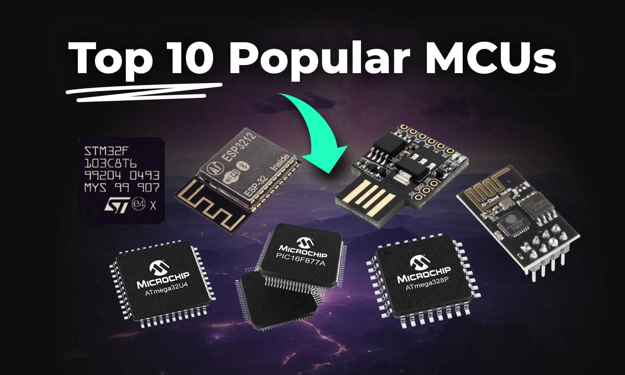
This article highlights 10 of the most popular microcontrollers, based on their usage in embedded systems, memory architecture, and the community support they enjoy.
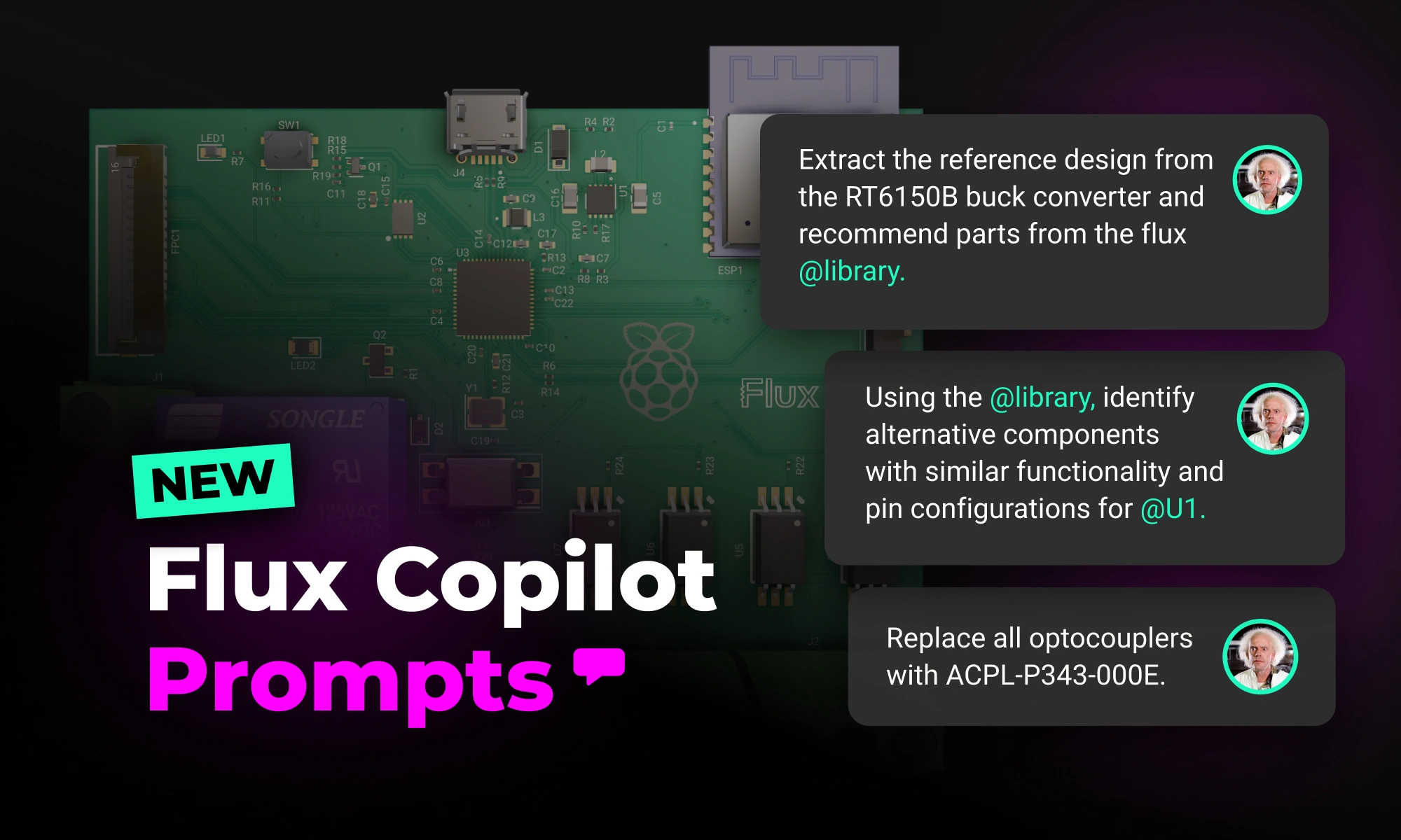
With the latest release of Copilot it isn’t just smarter—it’s hands-on, placing components and applying bulk changes to your project instantly. But to get the most out of it, knowing how to craft the right prompt is key.
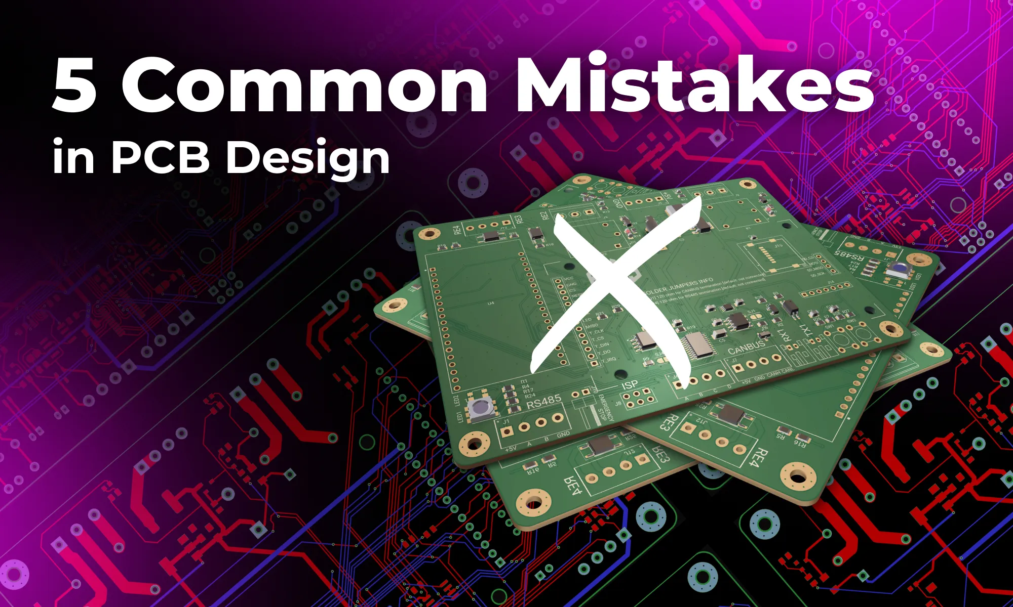
Avoid costly errors in your PCB design with these expert tips! Discover the 5 most common mistakes in trace width, vias, power planes, and more. Learn how Flux’s AI Copilot helps you catch these issues early, ensuring your board is ready for manufacturing.
This blog will explore functional block diagrams, their pivotal role in system design, the symbiotic relationship with ladder logic, structured text, and the broader realm of PLC programming. Why FBDs are so important within complex systems.
Delve into the essentials of circuit diagrams, exploring the various electronics symbols and their roles in design, while also offering practical advice for effective use of diagramming tools like Flux.