May 30, 2025
Design Buck Converters Like a Pro
Share
BuildWithFlux


At its heart, a buck converter is nothing more than three core elements working together to regulate a higher voltage to a lower voltage—and understanding these will make everything else click.
Here’s the simple math for a 12 V→5 V converter:

That 42 % duty cycle tells the MOSFET exactly how long to stay on each cycle so the LC filter averages out to 5 V.
Behind the scenes, a control IC monitors the output, compares it to an internal reference, and tweaks that duty cycle in real time to handle changing loads or input swings. But regardless of controller complexity, the switch + inductor + filter always remain the converter’s heart and soul.
Pick the wrong inductor, and you may face problems like overheating, excessive output ripple, or even core saturation that starves your load under sudden demand. To help you choose wisely, here’s what every beginner EE should know about inductor characteristics:
Pro tip: Choosing an inductor with a bit of extra saturation current rating and modestly lower DCR gives you valuable headroom during prototyping—preventing unexpected heat and ripple issues as your load conditions change.
A combination of MLCCs and a bulk cap covers ripple from kHz to MHz—get this wrong, and you’ll hear audible squeals or see output spikes.
Deep dive: MLCCs lose capacitance under DC bias and heat. And yes, they can sing! Ensure parallel MLCCs are carefully secured mechanically to mute piezo effects. Placing smaller-value capacitors first help to attenuate the high frequency singing in the larger smoothing caps.
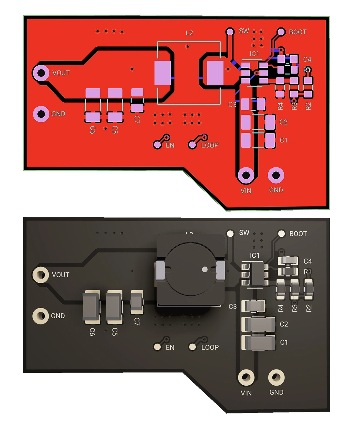
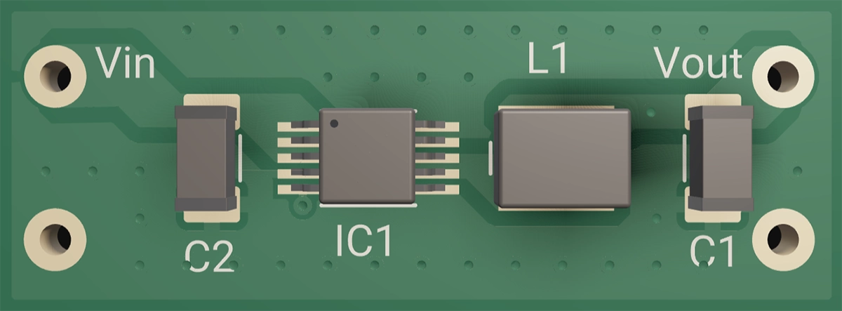
Having chosen your parts, layout is your next battleground. The difference between a noisy, inefficient converter and a clean, reliable one often comes down to copper placement. Follow these steps to keep that switching loop tight and your ground plane unbroken.
Remember: “Keep the switching loop tiny and the ground plane continuous.”
Minimize the Switch Loop
Separate Control Signals
From full DIY assemblies to one-click, ready-to-use modules, these different topologies trade off flexibility, board space, and time-to-market. Pick the one that fits your project rhythm.
Each template already includes polygon pours for power and ground, and via-stitching. Once cloned, customize only what matters.
Ground planes are a default in any Flux project, which reflows around all parts and pads to help with noise isolation. Polygons are now in Flux helping you leverage wide current paths for your output voltage to flow through. Adjust thermal reliefs, keep-outs, and copper weights without redrawing anything.
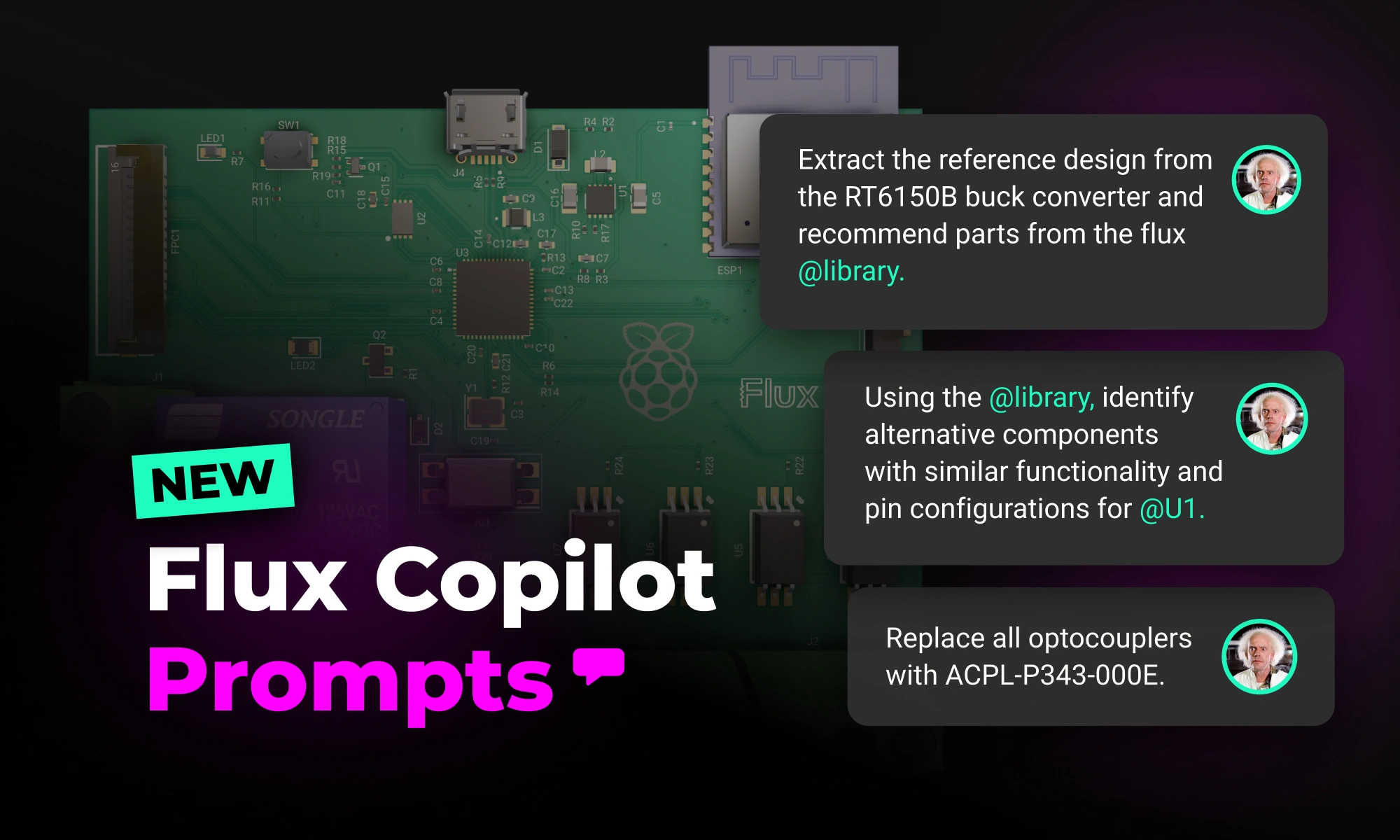
🤖 Copilot: Your AI EE Mentor:
Stuck on compensation loops or gate-resistor values? Ask Copilot right inside the editor. It explains theory, suggests values, and even pulls tables from datasheet PDFs.
🛣️ Auto-Layout for Non-Critical Nets:
Zone off low-speed signals—UART, I²C, sensors—and let Auto-Layout handle them. That frees you to hand-route the critical buck loops that define performance.
“Copilot help me determine the best orientation of U1 to minimize the switching current loop.”
Think of this as your design checklist: tape it to your monitor, keep it next to your keyboard, or fold it in your notebook. Pull it up whenever you need a formula, a layout reminder, or a topology refresher.
With Flux’s polygons, AI Copilot, and Auto-Layout, you’ll spend less time wrestling nets and more time optimizing your power stage—so you can ship faster and with confidence.
👉 Get started now » Open Flux and Clone a Buck Converter
At its heart, a buck converter is nothing more than three core elements working together to regulate a higher voltage to a lower voltage—and understanding these will make everything else click.
Here’s the simple math for a 12 V→5 V converter:
That 42 % duty cycle tells the MOSFET exactly how long to stay on each cycle so the LC filter averages out to 5 V.
Behind the scenes, a control IC monitors the output, compares it to an internal reference, and tweaks that duty cycle in real time to handle changing loads or input swings. But regardless of controller complexity, the switch + inductor + filter always remain the converter’s heart and soul.
Pick the wrong inductor, and you may face problems like overheating, excessive output ripple, or even core saturation that starves your load under sudden demand. To help you choose wisely, here’s what every beginner EE should know about inductor characteristics:
Pro tip: Choosing an inductor with a bit of extra saturation current rating and modestly lower DCR gives you valuable headroom during prototyping—preventing unexpected heat and ripple issues as your load conditions change.
A combination of MLCCs and a bulk cap covers ripple from kHz to MHz—get this wrong, and you’ll hear audible squeals or see output spikes.
Deep dive: MLCCs lose capacitance under DC bias and heat. And yes, they can sing! Ensure parallel MLCCs are carefully secured mechanically to mute piezo effects. Placing smaller-value capacitors first help to attenuate the high frequency singing in the larger smoothing caps.
Having chosen your parts, layout is your next battleground. The difference between a noisy, inefficient converter and a clean, reliable one often comes down to copper placement. Follow these steps to keep that switching loop tight and your ground plane unbroken.
Remember: “Keep the switching loop tiny and the ground plane continuous.”
Minimize the Switch Loop
Separate Control Signals
From full DIY assemblies to one-click, ready-to-use modules, these different topologies trade off flexibility, board space, and time-to-market. Pick the one that fits your project rhythm.
Each template already includes polygon pours for power and ground, and via-stitching. Once cloned, customize only what matters.
Ground planes are a default in any Flux project, which reflows around all parts and pads to help with noise isolation. Polygons are now in Flux helping you leverage wide current paths for your output voltage to flow through. Adjust thermal reliefs, keep-outs, and copper weights without redrawing anything.
🤖 Copilot: Your AI EE Mentor:
Stuck on compensation loops or gate-resistor values? Ask Copilot right inside the editor. It explains theory, suggests values, and even pulls tables from datasheet PDFs.
🛣️ Auto-Layout for Non-Critical Nets:
Zone off low-speed signals—UART, I²C, sensors—and let Auto-Layout handle them. That frees you to hand-route the critical buck loops that define performance.
“Copilot help me determine the best orientation of U1 to minimize the switching current loop.”
Think of this as your design checklist: tape it to your monitor, keep it next to your keyboard, or fold it in your notebook. Pull it up whenever you need a formula, a layout reminder, or a topology refresher.
With Flux’s polygons, AI Copilot, and Auto-Layout, you’ll spend less time wrestling nets and more time optimizing your power stage—so you can ship faster and with confidence.
👉 Get started now » Open Flux and Clone a Buck Converter


Discover our latest schematic design updates that streamline wire adjustments, component alignment, and intuitive pin connections, making your design process faster and meeting your high standards for precision. These enhancements, coupled with our AI design assistant, ensure a solid foundation for your projects.

Learn how smart vias in Flux automates the selection, placement, and configuration of vias during the PCB design process. This automation reduces the manual effort involved in via placement and significantly lowers the risk of misalignment and other common errors associated with traditional via management.

In this blog post, we explore how Flux.ai effectively uses Web Workers and ImmerJS to enhance data replication in our web-based EDA tool. We discuss our challenges with data transfer, our exploration of SharedArrayBuffer, and our ultimate solution using ImmerJS patches.

Discover how CAD Librarians can leverage Flux’s key capabilities—AI Part Imports, Component Updates, Live Pricing, and JEP30 Export—each tailored to meet the specific demands of maintaining PCB libraries.

This blog post highlights a series of innovative reference designs developed by renowned manufacturers using Flux. These reference designs encompass a variety of applications, including advanced light sensing, robust data communication, and compact distance measurement. This diverse array showcases the adaptability and effectiveness of Flux in meeting the varied needs of industrial sensing applications

A comprehensive guide to using solder flux in electronics soldering. Soldering flux is used to clean and prepare the surfaces of the components that need to be joined. It helps to remove oxidation and other contaminants that can prevent a strong bond from forming. Flux also reduces surface tension, allowing the solder to flow more easily and improves the wetting of the components.
With the latest release of Copilot it isn’t just smarter—it’s hands-on, placing components and applying bulk changes to your project instantly. But to get the most out of it, knowing how to craft the right prompt is key.
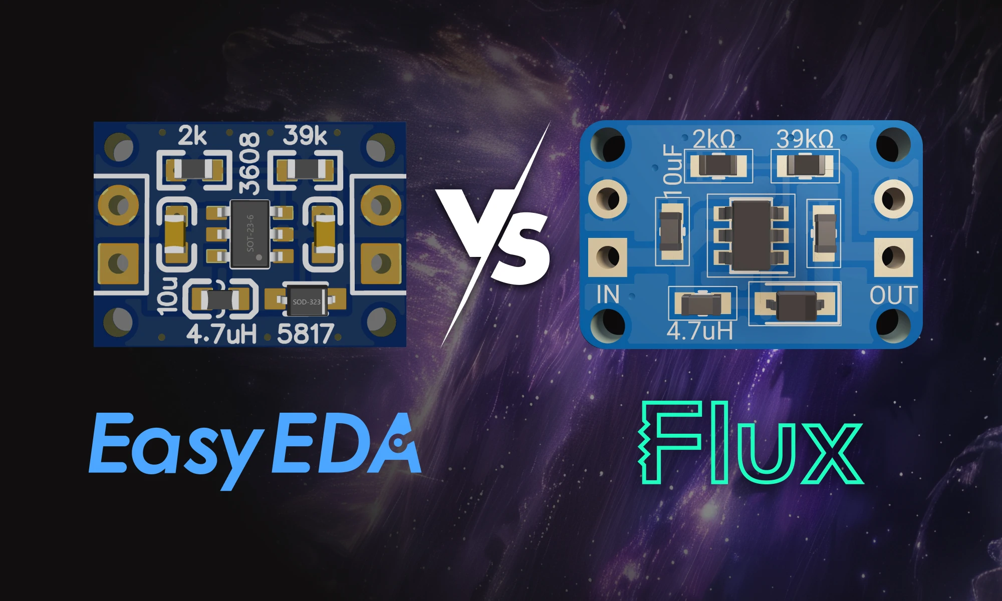
If you’re using EasyEDA and are thinking of making the switch to Flux, learn how the two platforms differ and why Flux might be the next step in elevating your PCB design experience.

One of the key components of PCBs are vias, which are tiny pathways that allow electrical signals to travel from one layer of the board to another. Vias are a staple of PCB design.

The blog post dives into the technical aspects of Multilayer Ceramic Capacitors (MLCCs), highlighting their importance in electronic circuits. It explains the construction of MLCCs, where layers of ceramic material and metal electrodes create a multilayered structure to store electrical energy.


Effortlessly calculate parallel and series resistor values with our accurate, user-friendly tool designed to optimize circuit performance and streamline electrical design processes.

Electronics, whether in a phone or an industrial motor, face potential threats from unchecked electrical currents. Our guide introduces protection circuits, the essential safeguards that monitor and respond to such electrical anomalies.